An infrared detector is simply a transducer of radiant energy, converting radiant energy in the infrared into a measurable form. Infrared detectors can be used for a variety of applications in the military, scientific, industrial, medical, security and automotive arenas. Since infrared radiation does not rely on visible light, it offers the possibility of seeing in the dark or through obscured conditions, by detecting the infrared energy emitted by objects. The detected energy is translated into imagery showing the energy differences between objects, thus allowing an otherwise obscured scene to be seen.
Under infrared light, the world reveals features not apparent under regular visible light. People and animals are easily seen in total darkness, weaknesses are revealed in structures, components close to failure glow brighter, visibility is improved in adverse condition such as smoke or fog.
Infrared Detector Formats
Infrared detectors are available as single element detectors in circular, rectangular, cruciform, and other geometries for reticle systems, as linear arrays, and as 2D focal plane arrays.
Single element infrared detectors are normally frontside illuminated and wire bonded devices. Linear and 2D arrays may be fabricated with a variety of device and signal output architectures.
First generation linear arrays were usually frontside illuminated, with the detector signal output connected by wire bonding to each element in the array. The signal from each element was then brought out of the vacuum package and connected to an individual room temperature preamplifier prior to interfacing with the imaging system display. Gain adjustments were usually made in the preamplifier circuitry. This approach limited first generation linear arrays to less than two hundred elements.
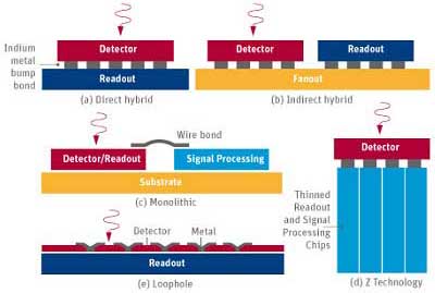
Second generation arrays, both linear and 2D, are frequently backside illuminated through a transparent substrate. Several alternative focal plane architectures are illustrated in the graph below.

Figure (a) illustrates a detector array which is electrically connected directly to an array of preamplifiers and/or switches called a readout. The electrical connection is made with indium “bumps” which provide a soft metal interconnect for each pixel. This arrangement, commonly referred to as a “direct hybrid”, facilitates the interconnection of large numbers of pixels to individual preamplifiers coupled with row and column multiplexers.
Indirect hybrid configurations (b) may be used with large linear arrays to interface the detector with a substrate having a similar thermal coefficient of expansion. These hybrids may also be used for serial hybridization, allowing the detector to be tested prior to committing the readout, and/or to accommodate readout unit cells having dimensions larger than the detector unit cell, increasing the charge storage capacity and thereby extending the dynamic range. Readouts and detectors are electrically interconnected by a patterned metal bus on a fanout substrate.
Monolithic detector arrays (c) have integrated detector and readout functions. Generally, in these arrays, the command and control signal processing electronics are adjacent to the detector array, rather than underneath. In this case, the signal processing circuits may be connected to the detector by wire bonds. In the monolithic configuration it is not necessary for the signal processing circuits to be on the same substrate as the detector/readout (as shown in the figure) or at the same temperature as the detector. Monolithic PtSi detector arrays can be made with signal processing incorporated on the periphery of the detector/readout chip through the use of silicon-based detector technology.
Z technology, as illustrated in figure (d), provides extended signal processing real estate for each pixel in the readout chip by extending the structure in the orthogonal direction. In the approach illustrated, stacked, thinned readout chips are glued together, and the detector array is connected to the edge of this signal processing stack with indium.
Finally, a “Loophole” approach, as illustrated in figure (e), relies on thinning the detector material after adhesively bonding it to the silicon readout. Detector elements are connected to the underlying readout with vias, which are etched through the detector material to contact pads on the readout and metallized.
Infrared detector types
Many of these infrared detector materials are based on compound semiconductors made of III-V elements such as indium, gallium, arsenic, antimony, or on the II-VI elements mercury, cadmium and telluride, or on the IV-VI elements lead, sulfur and selenide. They can be combined into binary compounds such as GaAs, InSb, PbS and PbSe or into ternaries such as InGaAs or HgCdTe.
| Photon detectors | Energy detectors | ||
|---|---|---|---|
| Intrinsic, PV | MCT Si, Ge InGaAs InSb, InAsSb | Bolometers | Vanadium Oxide (V2o5) Poly-SiGe Poly-Si Amorph Si |
| Intrinsic, PC | MCT PbS, PbSe | Thermopiles | Bi/Sb |
| Extrinsic | SiX | Pyroelectric | Lithium Tantalite (LiTa) |
| Photo-emissive | PtSi | Ferro-electric | Barium Strontium |
| QWIP | GaAs / AlGaAs | Micro cantilever | Bimetals |
What are Shortwave Infrared(SWIR) InGaAs Detectors?
Xenics has developed shortwave infrared InGaAs detectors that offer a spectral range of 0.4 – 1.7 µm, 0.9 – 1.7 µm, 1.0 – 2.2 µm and 1.0 – 2.5 µm. The very beneficial extension from 1.7 µm to 2.2 µm and 2.5 µm is accomplished by varying the fraction of indium in the ternary compound. Introducing indium into GaAs decreases the bandgap of the compound and enables the detection of infrared radiation of longer wavelengths. The graph below illustrates how the bandgap will change when the composition of the III-V compound changes. However, changing the composition of a compound material will also change the lattice constant of the material. Most IR materials are fabricated lattice-matched, meaning: on a substrate that has the same lattice constant as the IR material itself. For III-V compounds, the most commonly used substrates are GaAs, InP, InAs, GaSb and InSb. The InGaAs alloy with a 1.7 µm cut-off wavelength is lattice matched to InP. Therefore it is generally fabricated on InP substrates. In order to extend its sensibility to longer wavelengths, the alloy has to be fabricated on a lattice-mismatched substrate. This can be done on an InP substrate or on a standard GaAs substrate.
Using the lattice matched and mismatched technology, state of the art InGaAs linear arrays as well as focal-plane-array (FPA) detectors have been fabricated.

What is an Uncooled Bolometer?
An uncooled bolometer consist of thermally isolated microbridges, with a temperature sensitive material deposited on top. The temperature sensitive material can be V2O5, a-Si or poly-SiGe. The microbridges are surface-micromachined directly on the circuits.
Combining thermal detector elements with an integrated circuit raises the problem of interfacing the detector elements and the IC. One of the more serious problems arises because thermal detector elements must be heated, or allowed to cool, due to the radiation to be detected. Therefore, for optimum performance, the detectors must be thermally isolated from their surroundings. This precludes the simple depositing or mounting of the detectors directly on the IC – because Si is a good thermal conductor. Otherwise, the detectors would become so thermally loaded that it would adversely affect their performance as thermal detectors.
Therefore, the microbridges are surface-micromachined directly on the circuits. This permits the fabricating of contact supports that establish a compromise between a good electrical contact, which is needed to read out the detector element, and a poor thermal contact, which prevents thermal leakage of the absorbed radiation.